What are the Mainstream Integrated Circuit Design and Production Processes?

I. Introduction
Integrated Circuits (ICs) are the backbone of modern electronics, enabling the functionality of everything from smartphones to supercomputers. An integrated circuit is a set of electronic circuits on a small flat piece (or "chip") of semiconductor material, typically silicon. The importance of ICs in contemporary technology cannot be overstated; they are fundamental to the operation of virtually all electronic devices, driving advancements in computing, communication, and consumer electronics. This blog post will provide an overview of the mainstream design and production processes involved in creating integrated circuits, highlighting the intricate steps that transform ideas into functional electronic components.
II. Integrated Circuit Design Process
The design of an integrated circuit is a complex, multi-step process that requires a blend of creativity, engineering, and technical expertise.
A. Conceptualization and Specification
The design process begins with conceptualization, where engineers identify the requirements of the IC. This involves understanding the intended application, performance metrics, and constraints. Once the requirements are clear, specifications are defined, detailing the operational parameters, power consumption, and size constraints.
B. Architectural Design
Following the specification phase, the architectural design takes place. This high-level design phase involves selecting the appropriate architecture for the IC, which could be digital, analog, or mixed-signal. The choice of architecture significantly influences the performance and efficiency of the final product.
C. Logic Design
Once the architecture is established, the next step is logic design. This phase employs Boolean algebra and logic gates to create the necessary logic functions. Engineers design both combinational circuits (where the output is a function of the current inputs) and sequential circuits (where the output depends on past inputs as well).
D. Circuit Design
The circuit design phase involves schematic capture, where the circuit is represented visually. Engineers use simulation tools to verify the functionality of the design, ensuring that it meets the specified requirements. This verification process is crucial, as it helps identify potential issues before moving to the physical design stage.
E. Physical Design
The final stage of the design process is physical design, which involves creating the layout of the IC. This includes placing components and routing connections on the chip. Design Rule Checking (DRC) ensures that the layout adheres to manufacturing constraints, while Layout versus Schematic (LVS) verification confirms that the physical layout matches the intended design.
III. Integrated Circuit Production Process
Once the design is finalized, the production process begins, which involves several critical steps.
A. Wafer Fabrication
The first step in production is wafer fabrication. This process starts with the preparation of silicon wafers, which serve as the substrate for the ICs. Photolithography is then used to transfer the circuit patterns onto the wafer. This involves coating the wafer with a light-sensitive material, exposing it to light through a mask, and developing the pattern.
B. Doping and Ion Implantation
After photolithography, doping and ion implantation are performed to introduce impurities into the silicon. This process alters the electrical properties of the silicon, allowing it to function as a semiconductor. Precise control over the doping process is essential to achieve the desired electrical characteristics.
C. Metallization
Metallization follows, where interconnections between different components on the IC are created. Metals such as aluminum and copper are deposited onto the wafer to form the necessary electrical connections. This step is crucial for ensuring that signals can travel between different parts of the circuit.
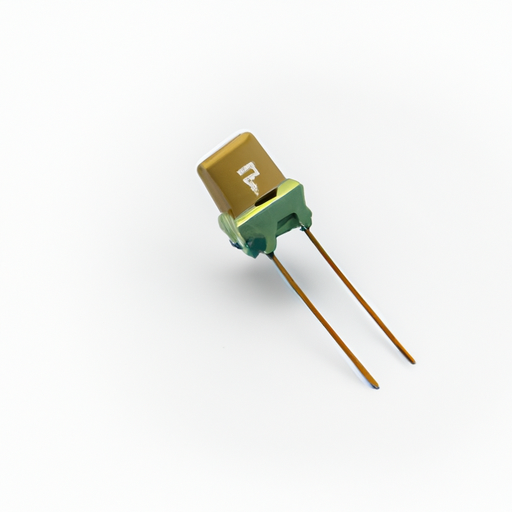
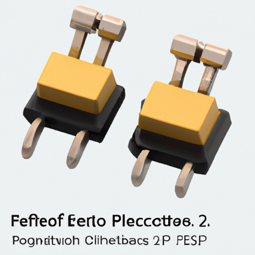
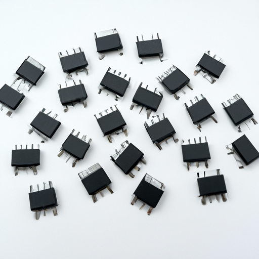
D. Packaging
Once the ICs are fabricated, they must be packaged to protect them and facilitate their integration into electronic devices. Various packaging types exist, including Dual In-line Package (DIP), Quad Flat Package (QFP), and Ball Grid Array (BGA). The choice of packaging affects the thermal and electrical performance of the IC, making it a critical consideration in the production process.
E. Testing and Quality Assurance
The final step in the production process is testing and quality assurance. Functional testing ensures that the IC operates as intended, while reliability testing assesses its performance under various conditions. Yield analysis is also conducted to determine the percentage of functional chips produced from a wafer, which is vital for assessing the efficiency of the manufacturing process.
IV. Challenges in IC Design and Production
Despite the advancements in technology, the design and production of integrated circuits face several challenges.
A. Technological Challenges
One of the primary technological challenges is miniaturization, often referred to as Moore's Law, which predicts that the number of transistors on a chip will double approximately every two years. As transistors shrink, issues related to power consumption and heat dissipation become more pronounced, necessitating innovative solutions to manage these challenges.
B. Economic Challenges
The economic landscape of IC production is also fraught with challenges. The cost of building and maintaining fabrication facilities is astronomical, often running into billions of dollars. Additionally, market competition and pricing pressures can impact profitability, forcing companies to continuously innovate and optimize their processes.
C. Environmental Considerations
Environmental concerns are increasingly relevant in IC manufacturing. The production process generates waste, and managing this waste is crucial for sustainability. Companies are exploring sustainable practices, such as recycling materials and reducing energy consumption, to minimize their environmental footprint.
V. Future Trends in IC Design and Production
The integrated circuit industry is evolving rapidly, with several trends shaping its future.
A. Advances in Design Automation
The integration of artificial intelligence (AI) and machine learning in design automation is revolutionizing the IC design process. Enhanced simulation tools are enabling faster and more accurate designs, reducing the time from concept to production.
B. Emerging Materials and Technologies
The exploration of new materials, such as graphene, is opening up possibilities for more efficient and powerful ICs. Additionally, the development of 3D ICs and system-on-chip (SoC) designs is pushing the boundaries of what is possible in integrated circuit technology.
C. Industry 4.0 and Smart Manufacturing
The advent of Industry 4.0 is transforming manufacturing processes, including IC production. The integration of the Internet of Things (IoT) allows for real-time monitoring and analytics, enhancing efficiency and reducing downtime in manufacturing facilities.
VI. Conclusion
In conclusion, the design and production processes of integrated circuits are intricate and multifaceted, involving a series of well-defined steps that transform ideas into functional electronic components. As technology continues to evolve, the importance of ICs in driving innovation and progress in various fields remains paramount. The ongoing challenges and future trends in the industry will shape the next generation of integrated circuits, ensuring that they continue to meet the demands of an increasingly digital world. The future outlook for the integrated circuit industry is bright, with advancements in design automation, emerging materials, and smart manufacturing paving the way for continued growth and innovation.